(Click image to download a PDF copy)
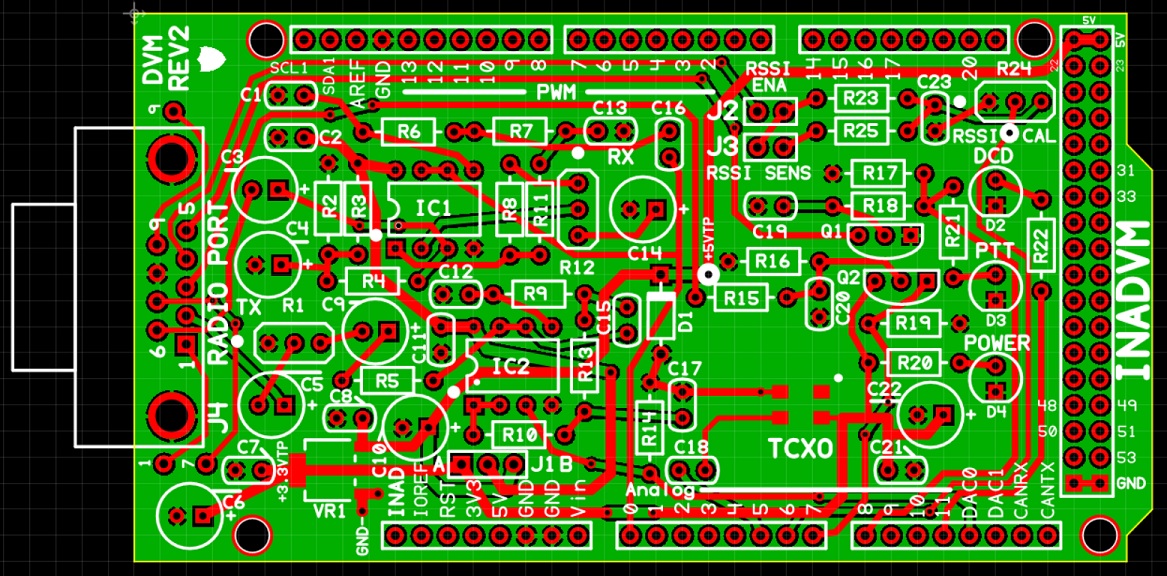
Board Depiction
(Click image for larger view)
Digital Voice Modem (audio filter and reference oscillator)
For Two-Way Ham Radio Applications
Documentation for the
INADVM REV2/3
Ordering instructions on bottom of page.
Board Depiction
(Click image for larger view)
Overview:
For several months now, a team of hams have been working on the development the INADVM.
Mike N4IRR, Steve N4IRS and I have been working on a line of MMDVM (like) audio boards called INADVM.
It is made and shipped from the USA. The first version of the board is for the Arduino Due.
It uses multi-turn pots for receive and transmit audio. The radio connector is a DB9. A 12 MHz TCXO is included.
On the board are LEDs for Power, PTT and Data Carrier Detect. Now for the fun part. The design is mostly through hole (not surface mount)
except for the voltage regulator and the TCXO. Those two parts are premounted the rest of the board is a kit.
You will receive the PC board with the regulator and TCXO mounted (and tested) and all the parts needed to complete it.
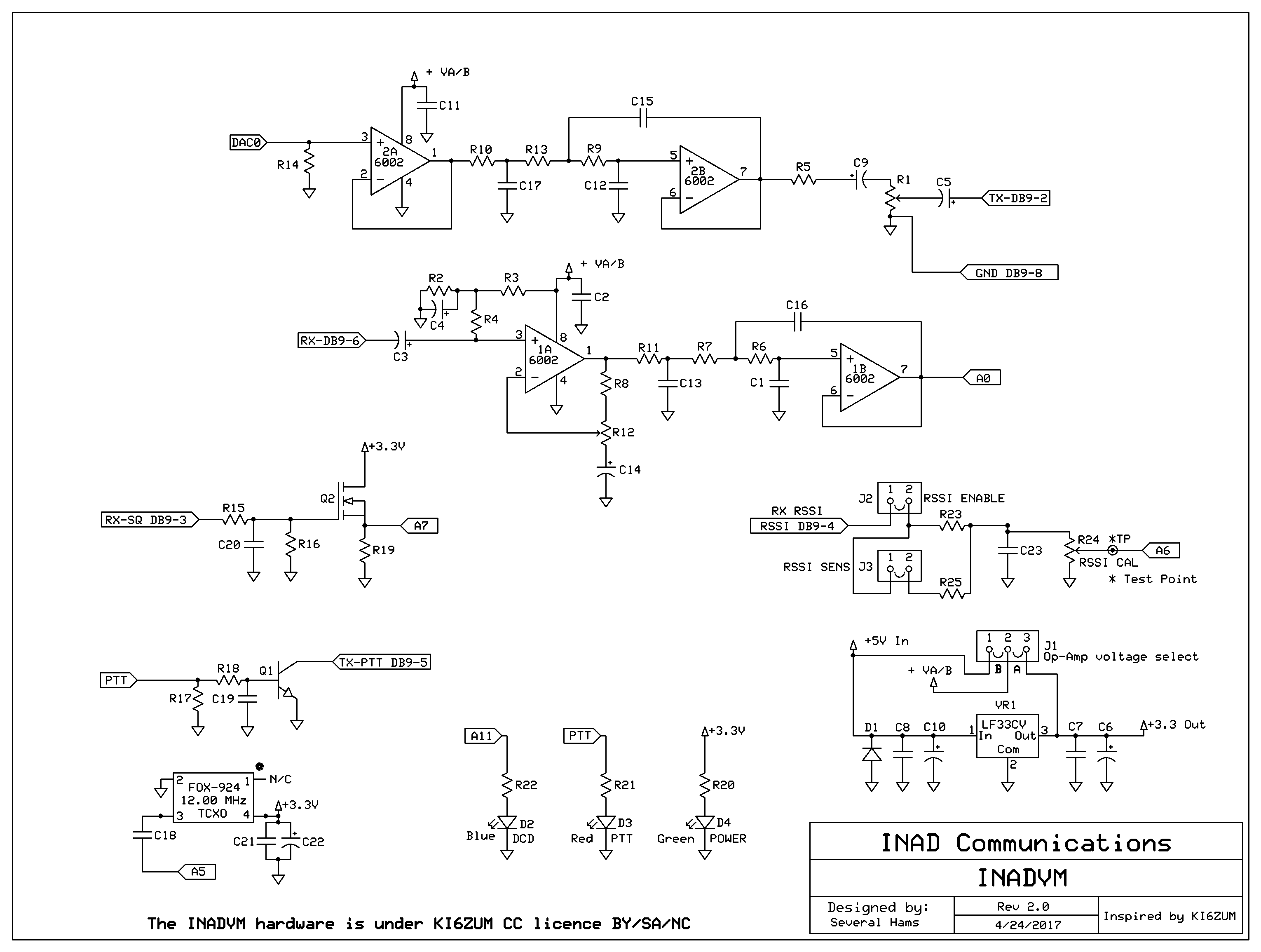
The schematic and board layout is available above. All ready to assemble. No surface mounted parts to solder.
Quality machine sockets for the ICs. There is an assembled version also.
We decided upon building a PC board that was mostly thru-hole instead of being like the other surface mount versions out there for several reasons, but mainly because the team saw other similar items be widely accepted because this form-factor is easier to build and modify by the average (ham) technician. There were about a dozen REV1 prototype INADVM's built and put through some rigorous beta testing. The results of this testing is what prompted changes and additions which makes up this latest revision production model.
If you purchased our kit, refer to the parts list and make sure you have all of the components
you need to build the kit. While all of them should be there - stuff happens.
Click here
for Parts List.
Construction/Assembly:
is NOT yet available for assembly
instructions and construction notes - with large photos. (Still needs written)
Click here for DB9 pin connection assignments.
Recommended powering requirements:
The board requires 5.0 VDC provided by the Arduino DUE.
Explanation of the logic signals and jumper pins:
The J1 header allows the audio filter op-amps to be sourced by 3.3 or 5.0 VDC. Position "A" is
normal, providing 3.3 volts to both filter amplifiers.
If this header is jumped to the "B" position, 5V is provided to the op-amps and
allows the circuitry to have a higher dynamic range and higher output level capability.
NOTE: If you are using a single INADVM
(for both RX and TX), it is recommended (and necessary) that you install the jumper into the 3.3 V position, as the resulting DC
offset (in the 5V position) will clip the RX path.
J2 and J3 on this production model are for RSSI. J2 enables RSSI, and J3 scales the sensitivity of the RSSI divider. The RSSI circuitry uses two fixed resistors and a mulit-turn potentiometer to scale the RSSI value. Any voltage between 3.4 and 15 VDC can be scaled to 3.3 volts. This is done by selecting the sensitivity of the divider. Lower RSSI voltages scale better with Jumper J2 installed, while higher RSSI voltages (above say 7.5 V) scale better with J2 removed. The INADVM's RSSI divider DOES NOT limit the voltage reaching the micro-controller (Due). However, a convenient test point is provided so yo can start out with the pot counter-clockwise (minimum voltage) and calibrate the RSSI output while receiving a 100% signal on the receiver.
The DCD input requires a logic high, and the PTT output is a logic low.
Difference between REV 2 and REV3:
There is very little functional difference between REV2 and REV3. The REV2 boards do not work correctly when JU1 is in the "B" or 5V position. While
the REV2 boards work fine on receive with JU1 in the B position, the offset created in the TX path creates undesirable distortion.
In REV3, the power jumper was reconfigured to allow the receiver audio path (only) to run at 5V instead of 3.3V. The REV3 TX path is unchanged with the setting of
jumper JU1 and remains at 3.3V in either case. The added capacitor (C24) is necessary when the jumper JU1 is moved from the 3.3V position to the 5V
position. Since there is probably no advantage of running the receiver path from 5V, we recommend using only the 3.3 volt setting of JU1 (JU1A) with either REV2 or REV3.
While it was a good idea, it's not very practical, as there's no real increase in dynamic range - since the Due can't handle any more than 3.3V on its input anyway.
REV3 boards started shipping by default since October 2017.
Secure PayPal Ordering - Use down arrow to make your selection.
Quantity can be changed at PayPal after pressing the "Add to Cart" button.
INADVM Ordering - Make a selection:
NO LONGER AVAILABLE
Email
Kevin Custer for ordering information, order by check, or orders to be shipped to other countries.
Product of INAD Communications, all rights reserved.
The INADVM hardware is under KI6ZUM CC license BY/SA/NC
Specifications may change without notice.
Designed by several hams.
Images are property of INAD Communications
Board layout by Kevin Custer W3KKC
HTML as of date below - All Rights Reserved!